Hi,
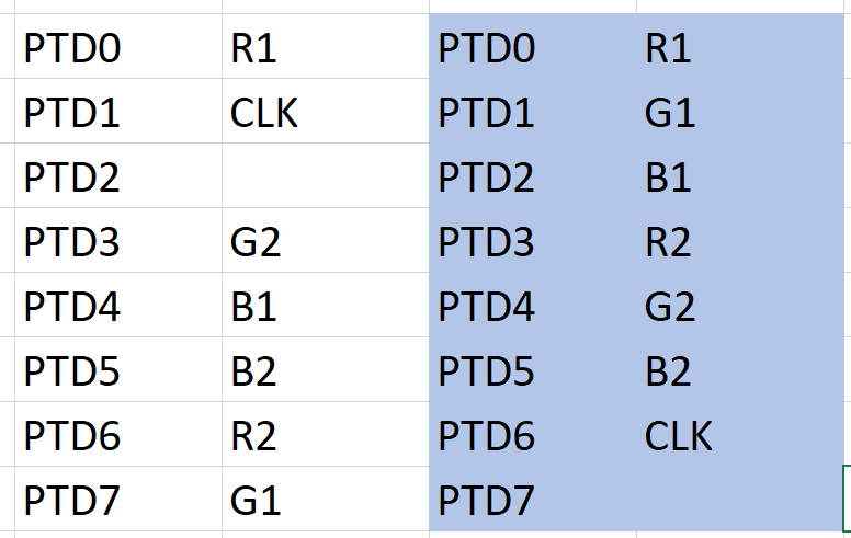
Is there a reason for the odd Pin mapping on the V4 Shield (see image below)? I would have thought that the mapping highlighted in blue would have made more sense, or does the V4 mapping help with mapping the rgb buffer to the DMA output buffer?
Note: i am just asking out of interest