Hello,
I am trying to map out a 64x64 hub 75 panel. These modules are made by LNSIN.
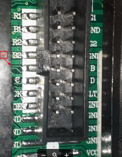
Here is a picture of the pinout of the panel that I am using:
There probably should be an “A” under “B2”, above “C”.
With ribbon cable plugged in:
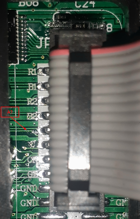
Here is how the ribbon cable is connected to the shield:
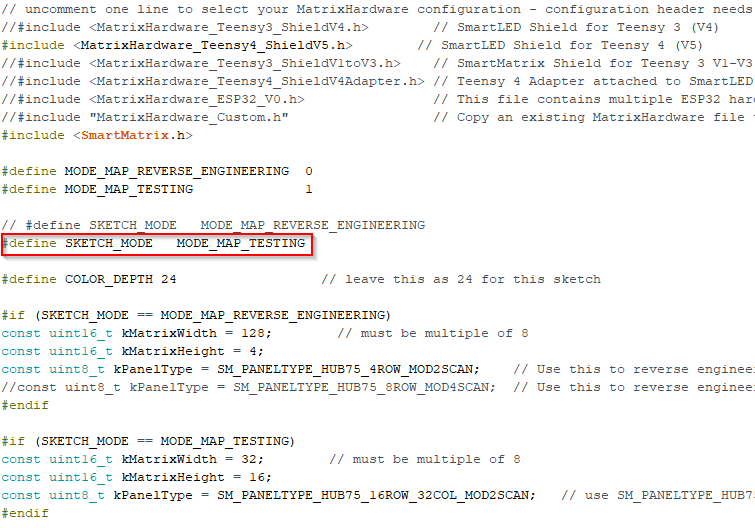
Reverse Engineering:
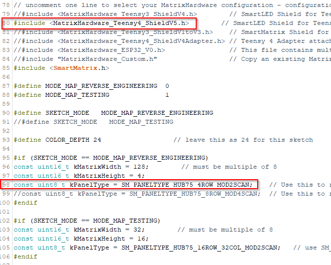
Here is the code that I set up before running the video:
Full video with the 250 ms delay:
I adjusted the delay to 1 instead of 250:
I don’t understand why we are using a 250 ms delay when the results here are faster and more clear when using a 1 ms delay instead.
Testing:
Then I change the sketch mode to testing:
And the output here is what I would expect in the reverse engineering mode. How would we know if this is a pass or fail?
Feature demo tests:
Now for the FeatureDemo with the same test settings:
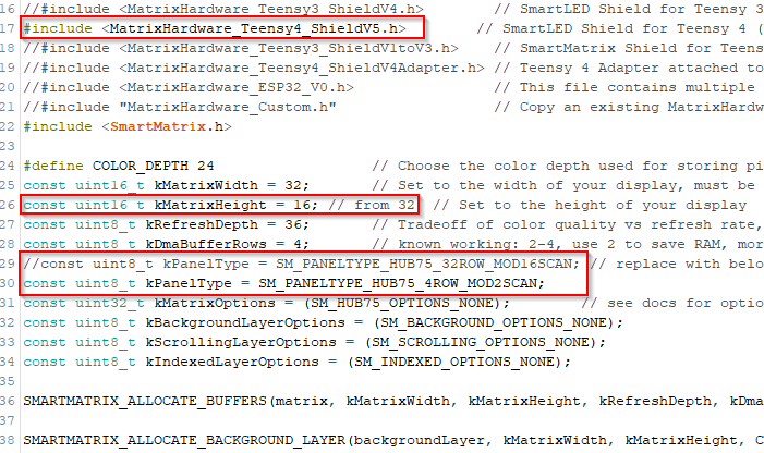
FeatureDemo output with test settings:
Must be that MOD2SCAN setting causing the 2 rows. I don’t understand why anyone would use this for anything practical.
Full video link:
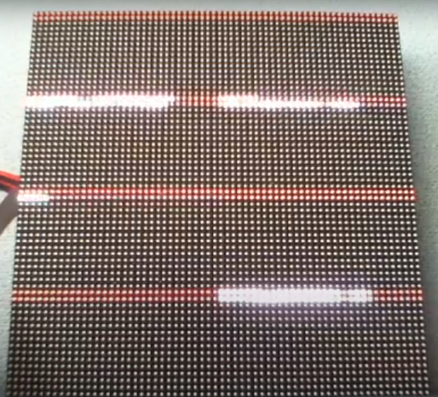
And after adjusting with the settings that work the best:
I thought I had it dialed in until about 2:52 seconds into the video, you can see a serious problem:

It is clearly seen that the 2nd “row” of “panels” is definitely out of place.
I didn’t notice at first because I thought it was part of the spectacular demonstration:
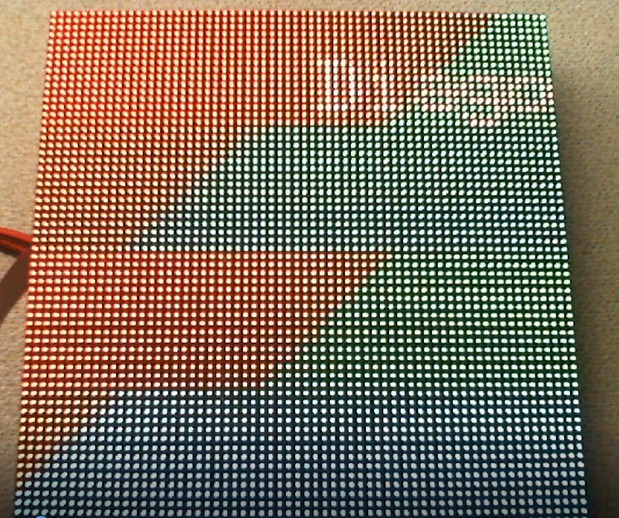
The problem is actually showing already here in the diagonal line demonstration. Looks like the 2nd and 3rd “row” are swapped.
Here is a link to the full video for the FeatureDemo:
Ultimately, I would like to get the mapping correctly so that the sections aren’t swapped. Maybe I’m wrong, but I believe that my mapping is wrong somehow.
What I would like to know is how I make a map from what is shown in the reverse engineering mode above. There doesn’t seem to be any pattern until I run it in test mode. In test mode, how would I know what to set it to? Isn’t the reverse engineering mode how you determine that?
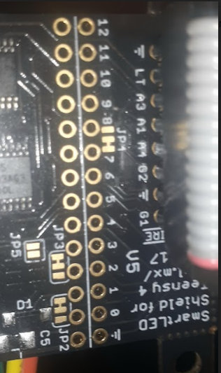
Also, Is it possible that the “skipped row” problem has something to do with the missing “A” on the PCB in the 1st diagram?
Update December 21, 2022, 1:00 pm EST
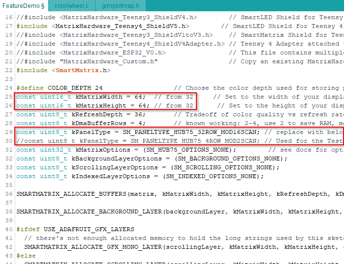
I have repeated the code above for clarity because I used it again for the next test.
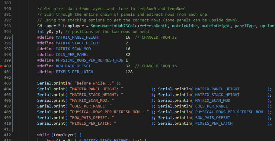
I modified the code in MatrixTeensy4Hub75Calc_Impl to print specific values when the code was appearing to swap panels 2 and 3. Then I took the output values and hard-coded them so that I could start modifying them until a combination that worked was found.
In the code shown below, I have changed MATRIX_PANEL_HEIGHT from 32 to 16 and ROW_PAIR_OFFSET from 16 to 32.
and the diagonal line test…

The panels line up perfectly and the remaining parts of the test seem to be working fine.
I have tried to change the code in MatrixCommonHub75.h, but when I change the MATRIX_PANEL_HEIGHT from 32 to 16 and ROW_PAIR_OFFSET from 16 to 32 I start getting garbage for output. I know that hard-coding these values is not the correct way to fix this, but I need a solution to work with for now.
Thanks,
EG
eg@americansjewelry.com